What the assembly floor covers
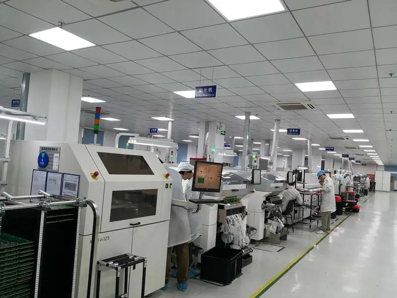
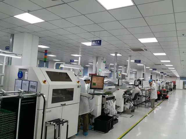
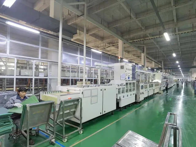
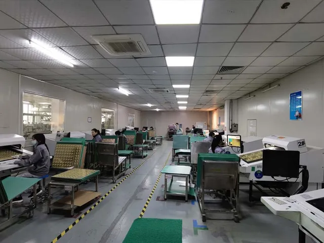
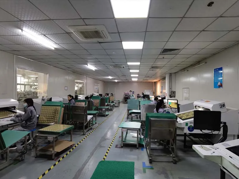
Hitech Circuits assembles printed circuit boards from single prototypes to volume production. Four SMT lines and three DIP lines run in the same plant as PCB fabrication, so component sourcing, board assembly, test and box build assembly stay inside one quality system — a fault found at functional test is traced back to the board, the part or the fit without another supplier in the loop.
Assembly processes
- Reflow soldering — the standard surface-mount process: solder paste is printed through a stencil, components are placed and the board is reflowed.
- Wave soldering — molten solder is pumped against the underside of the board to solder through-hole pins in a single pass.
- Selective soldering — a nozzle applies solder to individual through-hole joints, which keeps heat-sensitive neighbouring parts out of a second full thermal cycle.
- Hand insertion and soldering — still the right answer for odd-form parts, heavy connectors and rework.
- Point-to-point wiring — hand-mounted and soldered wiring for repair and legacy assemblies.
Parts can be placed on one or both sides at 4 mil (0.1 mm) pitch, down to 01005 and 0201 chip packages. Every process, and the inspection attached to it, is described on the printed circuit board assembly services page.
Where fabrication, parts and assembly are being sourced from China as one order, the China PCB assembly page explains how the four stages are quoted and traced together, and what paperwork ships with the order.
Engineering review before the first article
The Gerber set, BOM, pick-and-place file and assembly drawing go through DFM, DFA and DFT review: panel and stencil design, component clearance, polarity, test-point access and the placement program. Problems that would stop the line — a missing footprint, a part on stop, a package too close to a connector — are raised before the first board is built. First-article inspection then signs off every feeder, nozzle and vision setting on the run.
Inspection, test and rework
| Stage | What it catches |
|---|---|
| Solder paste inspection (SPI) | Paste volume, bridging and missed deposits before placement |
| Automated optical inspection (AOI) | Placement, polarity and solder defects after reflow |
| X-ray | BGA, micro-BGA, QFN and other joints hidden under the package |
| Ionograph | Ionic contamination left by flux and handling |
| In-circuit (ICT) and flying probe | Opens, shorts, orientation and component values |
| Functional test (FCT) | The board working against the customer test procedure |
Rework is done in-house, including BGA rework and re-balling verified by X-ray, so a board with one bad joint is repaired rather than rebuilt. The full gate list sits on the PCBA testing and quality assurance page.
Turnkey, partial turnkey and consignment
Three commercial models run on the same lines. In a full turnkey order the Gerber data and BOM are all that is needed — parts are sourced, boards fabricated, assembled, tested and packed. In a partial turnkey order the customer supplies the bare boards and selected components. In consignment assembly the customer supplies the components and everything else is handled here. The turnkey electronics assembly service covers the first two as one purchase.
Component supply is run by the components sourcing team, buying against the whole BOM and holding moisture-sensitive parts in temperature- and humidity-controlled storage; where a part is obsolete or on a long lead, a substitute is proposed before the schedule slips.
Which assembly service an order needs
The seven services are not a menu to pick from — the build data and the volume decide which of them apply, and one order can pass through three of them before it reaches series production.
- A design that has not been built yet belongs in express prototype assembly: the first article is checked on the line and the DFM findings go back into the layout while a change is still cheap.
- A released design with a repeating quantity belongs in low and high volume PCBA, where panelisation, feeder count and test coverage are set for the run rather than for the sample.
- Boards the customer already owns run as consignment assembly: bare boards and supplied parts are checked at IQC on arrival, and only the missing positions are sourced.
- A product that ships as a unit continues into box build assembly, where cable and harness work, enclosure fit and final test join the same inspection record.
- A board that fails in the field goes back through test and rework instead of a new build; the gates and the rework limits are listed on PCBA testing and quality assurance.
A quotation is revised when the order changes stage rather than when the customer asks, because a prototype package and a series package are priced on different cost lines.
What moves the price and the lead time
Two orders with the same Gerber set rarely quote at the same price, and placement speed is almost never the reason.
- Parts carry most of the cost. Distributor price breaks, whether a position comes from original manufacturer or franchised stock, and one long-lead part that forces a partial build move the quote further than the line does.
- Panelisation decides how long the line runs. Area lost on the panel is paid for on every board of the run, not once at tooling.
- Test coverage decided late buys a fixture. In-circuit test needs a bed-of-nails fixture built to the customer test points; where that decision lands after the order is placed, the fixture becomes a line item and a delay.
- A package with gaps restarts the clock. A BOM without manufacturer part numbers, an assembly drawing without polarity marks or a missing test procedure sends the order back to the customer before DFM begins, and the schedule restarts from the date the last file arrives.
The quotation is itemised along those lines, so when a budget has to come down it is visible which line to attack.
Getting a quotation
Send the Gerber set, BOM, pick-and-place data, assembly drawing, quantity and target date. A complete package is quoted within 24 to 48 hours; prototypes come back in 1–3 days and medium volume in 4–10 days, with stencils cut within four hours. Urgent prototype work runs through express prototype assembly and volume orders through low and high volume PCBA; process limits are listed on the capability page and the issued certificates on the certifications page.