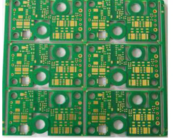
Heavy copper boards are built for current, not for signals. Increasing the copper thickness increases the cross-section of every trace, so the same trace width carries more current with less temperature rise, and the copper spreads heat sideways under the components. Copper conducts heat at 401 W/m·K, an order of magnitude above the laminate around it, which is why these boards turn up wherever a converter, motor or power stage has to survive its own losses.
Where heavy copper is used
- Power supplies and converters — primary and secondary sides of switch-mode supplies, bus bars and shunt paths.
- Motor drives and inverters — three-phase output stages in industrial control and pump drives where the current has to reach a connector without a cable.
- Automotive — 48 V systems, battery management, starter-alternator and charging hardware under IATF 16949:2016, described further on the automotive PCBs page.
- Renewable energy — solar micro-inverters, string converters and storage interfaces, where heat and current have to be handled on the same board; see renewable energy.
- Welding, plating and traction equipment — industrial current paths, covered on the industrial control page.
From 0.5 oz to 20 oz
One ounce of copper is about 35 µm, so the range runs from thin inner-layer foil up to roughly 700 µm on outer layers. Heavy copper normally means 3 oz (105 µm) and above per layer. Where a stack-up mixes a power layer with a fine-feature signal layer, the signal layer is held to the plant's 0.06 mm minimum line and space while the heavy layer's minimum is set by its copper weight and confirmed in the DFM review — etching a 20 oz layer is not the same process as etching a 1 oz layer.
What changes in the design
Copper weight affects more than resistance. Creepage and clearance distances grow, thermal reliefs have to be sized so a heavy pad can still be soldered by hand or by reflow, solder mask openings and via treatment are adjusted, and copper balance across the panel decides whether the finished board bows during lamination and reflow. The 15:1 aspect ratio and 0.15 mm mechanical hole minimum are the same as for standard boards, and impedance can be held to ±10 % on layers that need it.
Heavy copper, or a metal-core board?
Heavy copper and a metal-backed board both appear where a design is losing heat, and they are not the same answer. Heavy copper keeps the heat in the board: the thicker cross-section loses less in the first place and spreads what is left sideways under the components, so the board itself becomes part of the thermal path. An insulated metal substrate takes the heat out of the plane instead — the copper still carries the current, a thin dielectric isolates it, and the aluminium or copper base hands the heat to whatever the board is mounted on.
The first question is where the heat is allowed to go. In a sealed housing, on standoffs in still air, or where the current path is itself the source of the heat, heavy copper is the simpler answer because nothing has to leave the board. Where there is a chassis, a heatsink or a cold plate underneath, the vertical path is the one that matters and a metal-core build reaches it with less copper; the trade is that the dielectric has to stand off the voltage, so isolation becomes the limit rather than the conductor. Both constructions are described on the metal-core board page, and mixed designs are quoted together.
The second question is how much of the panel has to be thickened. Where the outline has room, widening the few nets that carry the current at a lower weight costs less than making every layer heavy; heavy copper earns its place when the cross-section has to fit a fixed width — a connector pitch, a slot in the housing, a busbar footprint — not simply when the current is large. Where the copper is also doing duty as a shield or as a low-inductance return, one layer answers two requirements and the case for it is stronger.
The third is assembly. A heavy layer holds a great deal of heat, so a joint on a power pad needs more energy and a longer soak than the fine-pitch parts sharing the board, and a reflow profile that suits one can starve the other. Where dense logic and a heavy current path cannot be separated in the layout, a multilayer signal section next to a separate power board is often cheaper than one stack-up asked to do both.
Assembly, test and documentation
Heavy copper panels run through four SMT lines at six million chips per day and three DIP lines at 1.6 million pieces per day, with reflow profiles set for the additional thermal mass. X-ray inspection covers joints under connectors, BGA rework and re-balling are handled in-house, and boards are fabricated to IPC-6012B and IPC-A-600H with UL recognition under file E354070.
Where a heavy copper build goes wrong
Most heavy copper problems are settled in the fabrication notes rather than on the etcher.
- Etch factor against finished width — thick copper is etched sideways as well as downwards, so the artwork width is not the finished width. The finished width and the tolerable undercut are called out on the drawing, and a coupon from the same panel is measured instead of assumed.
- Resin starvation at lamination — a heavy copper image leaves little room for prepreg to flow, so dielectric thickness and prepreg style are chosen together and bond strength is checked on the first panel; a dry laminate shows up later as delamination or as a conductive path between nets.
- Solder mask over a step — a heavy layer is a physical step in the surface, and mask that thins over the edge of the step cracks and bridges. Mask thickness and dam width are specified, and where a pad sits on the step the mask is plugged back rather than screened thin.
- Barrel plating against surface copper — plating current density follows the surface area, so a panel with heavy outer layers does not plate like a standard one. The minimum barrel copper is stated and a cross-section confirms it.
- Heat at the joint — the same copper that carries the current carries heat away from the soldering iron or out of the reflow zone, so thermal reliefs, preheat and dwell are agreed with the assembly process rather than left to the operator.
Getting a quotation
Send the Gerber set with the copper weight per layer, the current each net has to carry, the permissible temperature rise, board thickness and quantity. Prototypes come back in 1–3 days and medium volume in 4–10 days; the capability page holds the process limits and the certifications page the issued certificates.
Heavy copper boards that go on to assembly are covered on the China PCB assembly page, together with component sourcing and box build.