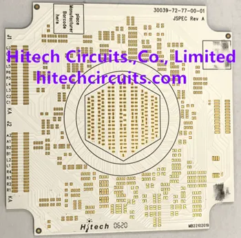
Ceramic substrates are used where the laminate is the limiting part of the design: a power module that has to shed its own losses, a laser or RF driver switching fast enough to heat its board, a sensor that must still insulate after a hundred thermal cycles. Ceramic carries both the heat and the voltage that FR-4 cannot, and Hitech Circuits builds those substrates in Shenzhen alongside the rigid, flex and metal-core lines.
Why ceramic instead of FR-4
- Heat — alumina runs 20–51 W/m·K and aluminium nitride 120–220 W/m·K, against roughly 0.3 W/m·K for FR-4, so the substrate spreads heat as well as carrying the circuit.
- Voltage — dielectric breakdown is 15, 20 or 28 kV/mm at 0.25, 0.63 and 1.0 mm thickness, which allows a thin piece to hold off a high working voltage.
- Temperature — parts see −55 to 850 °C, far past the glass transition of any laminate.
- Expansion — 7.4 ppm/K between 50 and 200 °C is close to the expansion of silicon and of most package materials, which keeps joint stress low on a large die.
- Stability — ceramic absorbs almost no moisture, so its dielectric properties survive humid plant conditions and repeated soldering.
Processes and materials
Direct copper bonded substrates are the usual choice for power: a copper foil is bonded to the ceramic at high temperature and then etched, which gives thick copper on a bonded interface. Thin-film and thick-film substrates are used where conductors and resistors are printed or deposited and where line definition matters more than copper weight; their conductors are AgPd or AuPd, while DCB uses copper only.
Alumina is the standard material, with 96 % and 98 % grades held in stock; aluminium nitride is chosen when thermal conductivity decides the design, and beryllium oxide where the highest conductivity is needed. Regular stock thicknesses run from 0.25 mm to 2.0 mm in sizes up to 130 × 140 mm, with thicker and larger pieces custom built and the largest alumina panel produced at 300 × 300 mm — the size tables are on the capability page.
Is ceramic the right substrate for the design?
Ceramic earns its price only where the substrate itself has to carry heat through a thin insulating layer:
- When a metal-core board is enough — if the losses reach the housing through a copper plane and a via field, an aluminium metal-core board is cheaper, comes in larger panels and takes outlines that a fired ceramic cannot.
- When the dielectric is the limit — an isolated bare die or a printed resistor network rules out both the laminate and the metal-core stack, because there the polymer does the insulating, not the substrate.
- When conductivity picks the grade — alumina is the default: cheapest to fire and able to carry thin- and thick-film conductors. Aluminium nitride is specified when the die cannot be cooled through alumina, and beryllium oxide is kept for the parts where neither of the other two survives.
- When the process picks the copper — a pattern that carries current needs the bonded copper of DCB; a part with printed resistors or a line definition finer than etched foil belongs in thin or thick film.
Where ceramic boards are used
Power modules and IGBT stacks, high-brightness LED and laser engines, RF and microwave stages, sensors for medical equipment that have to be sterilisable, and automotive power electronics that live next to the heat source. Where frequency rather than temperature is the problem, a high-frequency PCB on Rogers, Arlon, Taconic or Nelco laminate is usually the cheaper answer; ceramic becomes necessary when both requirements arrive together.
Where a ceramic substrate fails in service
The parts we are asked to analyse fail at the assembly and the outline rather than in the circuit:
- Cracks at a fixing point — ceramic has no yield, so a screw boss or a flexing clip starts a crack at the hole edge; keep fixing holes out of the stressed area, specify a washer and never let the substrate brace the housing.
- Delamination at the DCB interface — copper and ceramic expand at different rates, so a single large copper area peels from its edge after repeated cycling; break the copper into a mesh or segments instead of keeping it whole for layout convenience.
- Tracking along a cut edge — laser scoring and mechanical separation leave the conductor closer to the edge than the artwork shows; reserve a keep-out band at the outline and place the pattern inside it.
- Micro-cracks from the outline — an internal sharp corner concentrates the stress of every thermal cycle; radius the corners in the drawing and let singulation follow the radius, not the router bit.
Getting a quotation
Send the Gerber or DXF set with the ceramic material, the process, copper thickness, piece size and quantity. Because the conductor on a thin-film or thick-film part is deposited rather than etched, artwork and tolerances are reviewed in DFM before the quotation is fixed; the issued certificates are on the certifications page.
Ceramic PCB assembly service — SMT and through-hole on alumina, AlN and BeO substrates — is quoted together with fabrication on the PCB assembly page, with China-built boards covered on the China PCB assembly page.