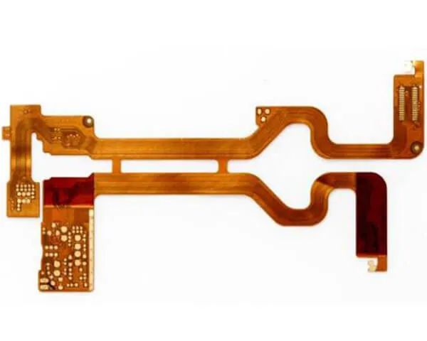
A flexible circuit carries the same conductor as a rigid board on a base that bends — polyimide, Kapton or PET, thin enough to fold into the space the product already has. That replaces a bundle of wires, the connectors at each end of it and the assembly time that goes with both, which is why handset, camera, wearable and medical designs are built on flex.
What a flexible circuit replaces
- Cable and connector assemblies — one flat circuit replaces the wiring harness and its two mating connectors, removing the joints that fail first in a moving product.
- Volume and weight — a 12.5–50 µm base with 12–25 µm coverlay weighs a fraction of an equivalent round cable and takes up no more room than its own thickness.
- Assembly time — the flex is placed and soldered like any other component, so a populated section that used to be hand-wired arrives as a single part.
- Dimensional freedom — the circuit can be routed in three dimensions, folded, and fixed to the housing with a pressure-sensitive adhesive.
Materials and stiffeners
PI, PET and Kapton base material covers most work, bonded to FR-4 where a section has to be rigid. Where a connector or a component needs a flat surface, PI, PET, FR-4 or stainless-steel stiffeners are laminated on, and the stiffener thickness is chosen together with the adhesive system so the finished part does not curl. Copper runs from 0.5 to 2 oz, and the finish is ENIG, immersion tin, OSP or carbon ink.
Is a flexible circuit the right choice?
A flex earns its place when the joint has to move, or when the housing leaves no room for a board, a connector and the stack of air between them. It is the wrong tool for an assembly that never moves: a rigid FR-4 board with one connector is stiffer, easier to rework and cheaper per part, and a short power run is still better served by a wire harness than by a circuit folded into place.
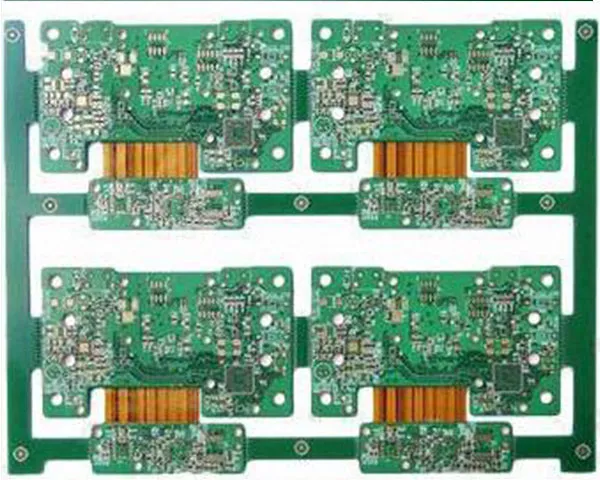
The three constructions answer different questions. A plain flex covers a single moving joint; a flex with stiffeners covers a joint that ends in a connector or carries a few components; a rigid-flex part is chosen when the same part number has to hold fine-pitch components on a section that cannot bend. Where the bend and the components sit apart, two parts joined by a connector usually cost less than one rigid-flex.
Price follows panel area and layer count rather than the shape of the outline, so a short circuit that folds once inside a small panel costs less than a long one snaking through the housing — and that decision is taken at layout, before a quotation is requested.
Design rules that decide the yield
Minimum line width and spacing are 0.002″ (3 mil) and the smallest hole is 0.006″ — finer than most cable-based designs need, but the bend area is what decides whether a flex survives. Conductors cross a fold at right angles rather than running along it, plating is kept out of the flexing region, coverlay windows are placed away from the bend, and the minimum bend radius is agreed at DFM so the copper is not compressed past its limit. Impedance can be held to ±10 % where the design is controlled-impedance, and HDI or rigid-flex constructions are used when the same circuit also has to carry fine-pitch components.
Where a flexible circuit fails in service
Most returns on flex trace back to four points, and each one is settled on the drawing or in the process sheet rather than by inspecting harder at the end of the line:
- Copper fatigue at the fold — a conductor that flexes repeatedly work-hardens and cracks at the trace edge, so a dynamic fold is specified on rolled-annealed copper and the bend radius is agreed at DFM.
- Coverlay lifting at a window edge — adhesive flows during lamination, so windows and stiffener edges are placed clear of the bend and the coverlay overlap is written into the drawing.
- A connector pad lifting after mating — the stiffener has to extend past the pad row and its thickness is agreed with the connector drawing; a short stiffener passes first article and fails in the field.
- Blistering after reflow — polyimide takes up moisture, so panels are baked before assembly and kept dry until the profile starts, with the reflow profile set for a thin, low-thermal-mass part.
Where flexible circuits are used
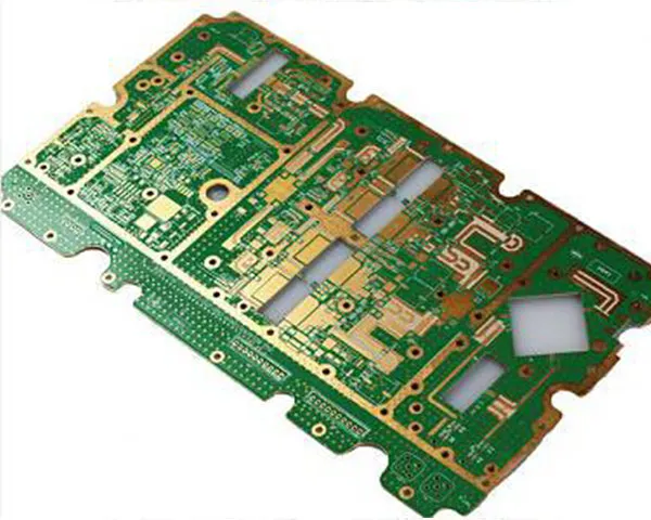
Mobile and wearable devices, camera and battery modules, medical equipment probes and monitoring patches, printers and moving heads in industrial control, and antenna and RF sections of telecommunications equipment. Where a rigid section is needed for the connector or the processor, a rigid-flex board puts both halves on one part number.
Getting a quotation
Send the Gerber set with the layer count, base material, copper weight, stiffener size and the bend radius the part has to survive. Assembly runs in the same plant, so a fully populated flex can be quoted as one order; the process limits are on the capability page and the issued certificates on the certifications page.
Flex circuits that continue into assembly are quoted with fabrication, sourcing and box build on the China PCB assembly page.