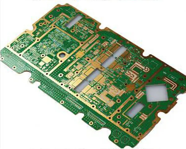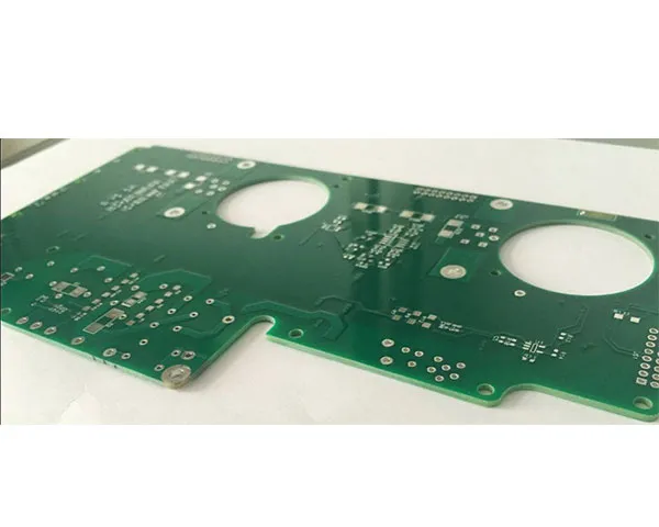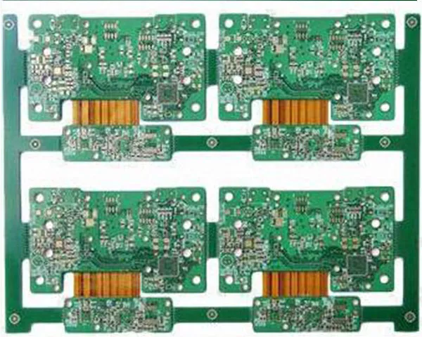
A rigid-flex board splits the work between two materials: the dense, well-supported sections stay on FR-4, and the connection between them is made on polyimide that folds into the shape of the housing. The flex is designed to sit at a fixed deflection — it is formed into its curve during fabrication or assembly, not left to flex through the life of the product.
What the construction removes
- Connectors — the mating connector pair and the flex-to-board interface disappear, so there are fewer parts to buy, stock and place.
- Signal path — transmission becomes rigid board to flex to rigid board instead of rigid board to connector to flex to connector to rigid board. Fewer changes of medium means less attenuation at the interfaces, which helps products that depend on signal accuracy.
- Assembly — fewer components cut SMT and unit-assembly man-hours, and fewer part numbers cut the management and inventory that goes with them.
- Reliability — the joints that fail first in a plug-and-socket connection are not there at all.
How a rigid-flex board is built
The flex core is fabricated first. FR-4 and prepreg are drilled and browned, the lay-up is riveted and pressed in a single cycle — copper-clad laminate, prepreg, the finished flex core, prepreg, top laminate — and the panel is then trimmed and measured for expansion and contraction, because polyimide moves and the registration of every later layer depends on it. Drilling, plasma de-smear, copper deposition and pattern plating follow, then outer-layer imaging, solder mask, finish, electrical test, punching and final inspection.
Design and cost trade-offs
A rigid-flex board costs more than a separate flex plus a rigid board, and the gap can look large before the connectors, the assembly labour and the inventory it removes are counted. A carrier is often needed to hold the flex sections flat through SMT and reflow, which adds assembly cost; bend regions are kept free of plated through-holes, stiffeners are used where a connector has to stay flat, and the layer count, copper weight and stack-up symmetry are set so the panel stays flat after pressing.
Where the rigid section ends and the flex section begins
On a rigid-flex drawing the decisive choice is not the layer count but the line where the two halves meet and what crosses it. The layer count, the press sequence and the carrier all follow from that line, which is why it is settled on the stack-up drawing long before the panel is tooled.
- The boundary is a material transition, not a line on paper. Where the flex core leaves the rigid stack the coverlay and the adhesive stop, the copper has to run without a plated hole and without a sharp corner, and the traces cross the bend line at right angles rather than running along it. A conductor that changes width at that point concentrates the strain in one place.
- How often the board folds settles the class of the design. A section formed once during assembly and then left in place carries a different construction from one that keeps moving: a static fold tolerates a thicker coverlay and a tighter radius, while a continuously moving one needs thinner base and cover film, a wider radius and no stiffener anywhere inside the bend.
- Stiffeners belong where the parts sit. Every connector and every SMT package has to land on the rigid section or on a stiffened area, otherwise the solder joint itself becomes the hinge and the movement is applied to the one place that cannot take it.
- Layer count is set by the bend region, not by density. The flex section usually keeps the fewest layers while the layers accumulate on the rigid side, so the flex core is built and tested first and the rigid stack is laminated around it — and where the rigid side is dense enough to need laser-drilled vias, that side follows the HDI PCBs route.
- The bend needs relief. A coverlay opening, a generous outline and a short free length at the transition give the copper somewhere to move; a flex section cut flush against a rigid edge tears at the corner.
None of this is a choice the quotation can make on the design's behalf. It changes the drill program, the press cycles, the carrier and the electrical test, so it is decided in the engineering review — the same place where the layer count on the rigid side is fixed.
Where rigid-flex boards are used
Handheld and smart devices, camera modules, medical equipment such as implantable and monitoring devices where space and weight decide the design, and security and control systems with a display or a sensor on a moving part. Where the circuit bends continuously but does not need a rigid section, a flexible PCB is the simpler answer.
What drives the price of a rigid-flex build
Two quotations for one rigid-flex drawing can differ widely with neither supplier wrong, because the price follows how many times the stack passes the press, how the flex sections are held through assembly, and how much of the order has to be built twice — not the finished board area.
- The flex core is a separate board before it becomes part of one. It is built, inspected and tested on its own panel, then laminated into the rigid stack, so a rigid-flex order carries two builds and two sets of yield losses instead of one.
- Every press cycle is another pass through lamination, drilling and registration. A stack with buried layers, or a board with rigid sections on more than one side, is pressed more than once, and the polyimide moves at each cycle, so the setup and the registration checks are paid again; where that count comes from is set out on the multilayer PCBs page.
- Carriers are tooling, not packaging. The flex sections have to be held flat through solder-paste printing, SMT and reflow, the carrier is built to this panel, and at a small quantity its cost lands on few boards — which is why it is usually charged as a one-off item rather than spread over the unit price.
- Stiffeners and coverlay are bonding steps of their own. Each polyimide, PET, FR-4 or stainless-steel stiffener has its own attach and cure, and a stack of them means stacked steps, so the stiffener set on the drawing is read as cost rather than as a footnote.
- The board is tested before and after lamination. The flex core is checked on its own panel, the finished board is checked again after pressing, plating and finish, and a bend check on the finished part needs its own fixture per design — a cost of the design rather than of the quantity.
Comparability comes down to the same list in reverse: the same layer count on each side, the same laminate family, the same fold class, the same stiffener set, the same carrier and panelization, and the same quantity. The limits behind each of those axes are on the PCB manufacturing capabilities page.
Getting a quotation
Send the Gerber set with the stack-up, the rigid-to-flex ratio, the bend radius and the layer count. Prototypes come back in 1–3 days and medium volume in 4–10 days; the process limits behind the quotation are on the capability page and the issued certificates on the certifications page.
Rigid-flex boards that continue into assembly are covered on the China PCB assembly page, including sourcing and box build.