Seven processes on one floor
Every board that leaves the plant has passed through at least one of these, and most pass through several:
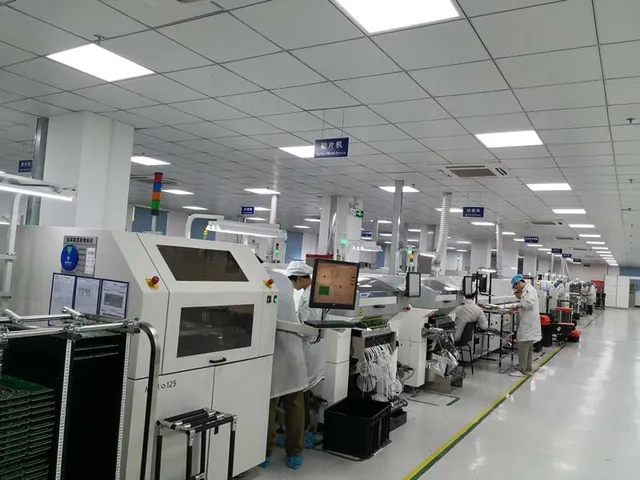
- Automated assembly — pick-and-place on four SMT lines, placing six million chips per day down to 01005 and 0201 packages at 4 mil (0.1 mm) pitch, on one or both sides of the board.
- Reflow soldering — paste printed through a stencil, parts placed, then soldered in a controlled profile for fine-pitch and area-array devices.
- Wave soldering — for through-hole and mixed boards where the pin count makes hand work uneconomical.
- Selective soldering — for connectors, terminals and other parts that must not see a full wave, or on boards where the through-hole joints sit next to parts that cannot be immersed.
- Hand insertion and hand soldering — for parts no machine can place, and for the low volumes where a fixture would cost more than the labour.
- Point-to-point wiring — internal wiring between boards, connectors and terminals inside an assembly.
- Inspection — SPI before placement, AOI after reflow, X-ray for BGA, QFN and other hidden joints, and ionograph testing of ionic contamination down to ppm per square centimetre.
Inspection and rework attached to each process
Inspection is not a final gate that a batch either passes or fails. Each process carries its own check, so a placement error is caught before reflow and a soldering error before the board moves on. Rework follows the same route: BGA and micro-BGA parts are reworked and re-balled on site and verified by X-ray, and contamination that could cause electrochemical failure later is measured and removed rather than assumed away.
Where a customer needs evidence for their own quality file — automotive, medical or industrial programs — inspection results are recorded against the lot, so the program can show what was checked and which process produced it.
Assembly and everything around it
PCB assembly is offered as a standalone service and as part of a turnkey build:
- Quick-turn prototype assembly for one to fifty boards.
- Turnkey and partial turnkey assembly covering fabrication and parts as well as the assembly work.
- Consignment assembly, where the customer supplies the components.
- Component sourcing, so a complete BOM is quoted and bought as one order.
- Inspection and test from SPI and AOI through to in-circuit, flying probe and functional test.
- Box build and final product assembly, including conformal coating and packing.
How a build moves through the plant
Component sourcing → PCB fabrication → SMT → DIP → testing → finished product assembly. Keeping those six stages on one site removes the freight, re-packing and re-inspection that come with splitting a build across suppliers, and it means a defect found at test can be traced back to the process that produced it rather than to an anonymous shipment.
RoHS-compliant lead-free assembly is the default; non-RoHS assembly is run where a customer's design or market requires it. Process limits for a specific design are on the capability page.
Choosing the soldering route for a board
A bill of materials does not name a route. What decides it is the mix of packages on the board, the board itself, and how many of them will be built.
- Surface mount only, no through-hole. One reflow, or two when both sides carry parts. A second reflow puts the board through a profile twice, so the first side has to survive the second pass — heavy thermal mass, aluminium electrolytics and moulded connectors are the parts that fail that test.
- A handful of through-hole joints. Hand soldering or a selective nozzle settles it, and what decides between them is not the pin count but whether the joints sit in one area or are spread across the board.
- Through-hole work across the whole board. Wave soldering becomes the cheaper answer once the pin count reaches the point where hand work stops paying for itself.
- Parts that must not see a wave. A connector whose housing softens at solder temperature, a plastic terminal block, an already-fitted display — the full wave is closed to them, so the route becomes selective soldering or a pallet that masks them out of the solder.
- Very uneven thermal mass. A board with a heatsink pad and heavy copper at one end and fine-pitch parts at the other is profiled for its most demanding point, which overcures everything else. Splitting it into two passes, or soldering only the through-hole joints selectively, is usually how such a board gets built.
- Volume decides the tooling. A stencil, a placement programme and a fixture have to be paid for, so on a small lot hand work can be cheaper than a line setup; past a certain quantity the same fixture turns into the saving rather than the cost.
The route is settled at the DFM stage, not once the line is already running. Stencil apertures, panel orientation, shadowing between tall parts, the masking pallet and the hand-soldering sequence all belong to that stage, and changing any of them afterwards means new tooling, a re-tuned programme and a fresh first-article record. Test points follow the same rule from the other side: where a joint cannot be reached once the route is fixed, it is the route that has to change, not the PCBA testing and quality assurance that comes after it.
What the soldering route costs, and what it saves
Two routes for the same board rarely differ by a rate per joint. They differ in how the cost is shaped: tooling paid once, labour paid per board, and the expected cost of rework.
- Tooling is fixed, labour is variable. Stencils, placement programmes, selective nozzles, masking pallets, hand-soldering fixtures and first-article records are paid once and carried by the lots that follow. A programme released in small batches therefore pays that block again on every release, which is why the price per board stops falling until the quantity does.
- Hand assembly is cheap to start and expensive to scale. It carries no tooling, and its cost sits in hours that grow with every board. What an hourly rate does not show is consistency: two operators produce two joint profiles, AOI and X-ray coverage is thinner behind them, and the record of who soldered what at which setting is what an audit asks for first.
- A wave is fast, a selective nozzle is precise. The wave needs the masking pallet and exposes the whole board to solder temperature; a selective nozzle touches only the joints it is aimed at, protects the parts beside them and usually returns fewer boards to rework.
- A second reflow is a second thermal budget. Double-sided surface mount spends the parts' heat allowance twice, and where that rules the parts out, the route quietly becomes hand soldering on the second side — which reads as a saving on the quotation and appears as labour on the floor.
- Changing the route reopens the clock. Once the line is running, another route means new stencils or a new pallet, a re-tuned programme and a fresh first article, so the price and the delivery date are restarted rather than adjusted.
- Two quotations compare only on the same route. Same sides, same through-hole method, same test coverage, same delivery terms — the volume page sets out what else moves a repeat order, and the process limits behind any route are on the capability page.