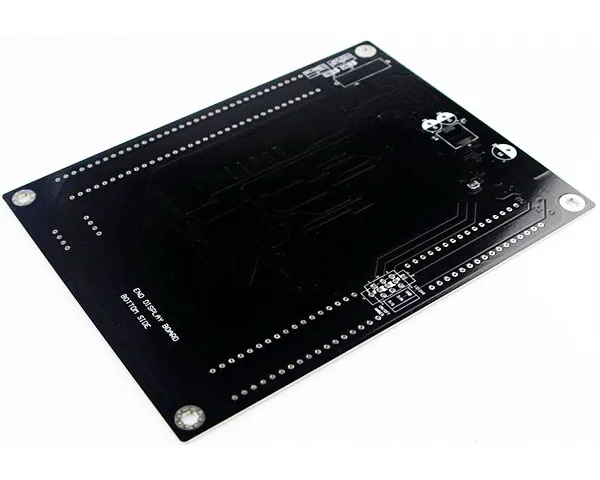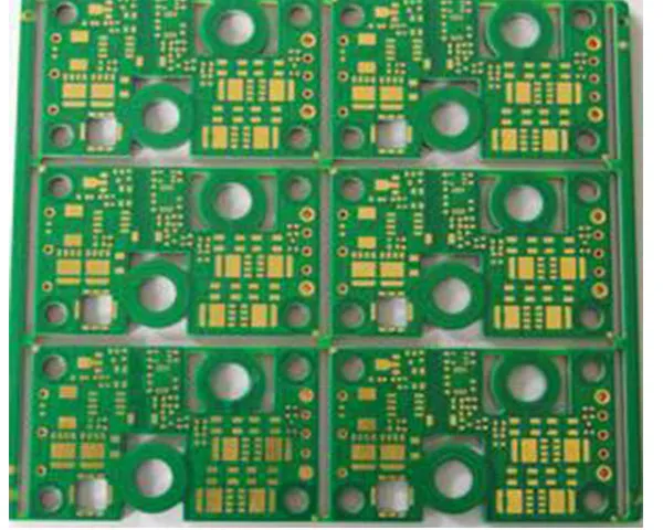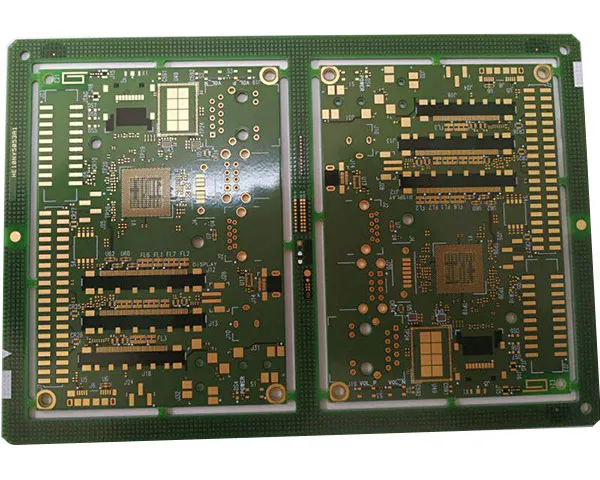
A conventional multilayer board connects its layers with mechanically drilled holes that pass through the whole panel. An HDI board drills the outer layers with a laser instead, so the connection only travels as far as it needs to. That releases the space a through-hole barrel would have occupied: more components fit in the same outline, the return path under a fine-pitch package gets shorter, and a board that would have needed extra layers stays thinner and lighter.
Stack-ups built here
- 1+N+1 — one microvia layer on each side of a mechanically drilled core, the usual first step up from a conventional multilayer board.
- 2+N+2 and 1+1+N+1+1 — two microvia layers per side, for fine-pitch BGA escape routing and denser connector fan-out.
- 3+N+3 — three microvia layers per side, where package pitch and pin count leave no other option.
- ELIC — every layer interconnected by microvias, without a mechanical core carrying through-holes.
Microvias are stacked directly on top of each other or staggered, and where a via sits inside a pad it is copper filled and capped so the pad stays flat for the paste deposit.
HDI or a conventional multilayer?
HDI is a routing answer, not an upgrade in itself. The useful question is whether the design has run out of room at the layer count the product can still carry. Take the escape routing first: if the fine-pitch packages and the connector fan-outs clear on the outer layers of a conventional build, adding signal layers is usually the cheaper path, because every microvia layer brings its own lamination, laser drilling and planarisation steps with it.
Thickness is the second test. Where a product is defined by its outline rather than by its circuit, microvias put more interconnect into a thinner board, which is what handheld, wearable and camera designs are built around. The third is the return path: a microvia stops at the layer it serves, so the loop under a high-speed bus shortens even when the layer count stays put — something extra copper on a conventional board cannot buy.
Where one design mixes a dense logic area with a power section that needs heavy copper, or where the density comes from a flex-to-rigid transition rather than from a fine-pitch package, the stack-up is reviewed next to the rigid-flex and multilayer builds before the quotation is fixed.
Microvias, drilling and plating
Microvias are laser drilled at 0.1 mm minimum, with mechanical drilling covering 0.15 mm and above at a 15:1 aspect ratio. The outer layers carry 0.06 mm line and space and copper from 0.5 oz to 20 oz, so a dense logic area and a power section can share one stack-up. After plating, the stack-up is imaged, laminated and inspected layer by layer; board profile, bow and twist and copper balance are checked against the same tolerances as the rigid line.
Materials and impedance
High-Tg FR-4 covers most HDI work, with halogen-free laminate where a customer's own approvals ask for it and Rogers, Arlon, Taconic or Nelco where the signal has to survive at high frequency. Impedance is held to ±10 % on 0.06 mm features, which is what makes dense HDI boards usable for high-speed buses as well as for miniaturised products; the same layer count in a multilayer PCB would need a larger board.
Where HDI boards are used
Consumer electronics, handheld and secure devices, security and camera systems, medical monitors and imaging, and automotive sensor and radar modules under IATF 16949:2016. Assembly runs on the same site — four SMT lines at six million chips per day down to 01005 parts, X-ray inspection and BGA rework — so the microvia under a BGA pad is inspected by the same team that placed the component.
Where an HDI build goes wrong
Most HDI problems are settled in the stack-up drawing rather than on the line.
- Stacked microvias and layer-to-layer registration — each microvia layer is drilled and imaged against its own targets, so a stacked via carries the offset of every layer below it. Staggered placement, target marks kept in the panel border and a via position that leaves margin inside the pad keep the last layer on the pad instead of beside it.
- Copper fill and the dimple under a pad — a filled via that is not planarised leaves a shallow depression, and the ball over it reflows into the gap. Fill and cap are specified explicitly and the paste aperture under the pad is checked against the via diameter.
- Lamination cycles against finished thickness — every added microvia layer is another press cycle, and the dielectric lost each time adds up. Thin products show it first, so dielectric is reserved per cycle in the stack-up and the finished thickness is quoted with its tolerance band.
- Via bottom condition — resin smear or an oxidised target pad at the bottom of a laser via raises the resistance of a connection that still passes continuity. Desmear and the via bottom treatment are named in the process notes, and a coupon from the same panel is cross-sectioned.
- Test access — microvias and filled pads occupy the space a test point would have used, so coupons, test points and boundary-scan access are planned with the stack-up rather than added once the layout is signed off.
Getting a quotation
Send the Gerber set with the intended stack-up, the finest pitch to be routed, impedance requirements and quantity. Prototypes come back in 1–3 days and medium volume in 4–10 days; process limits are listed on the capability page and the issued certificates on the certifications page.
HDI stack-ups that continue into assembly are quoted with sourcing and box build on the China PCB assembly page.