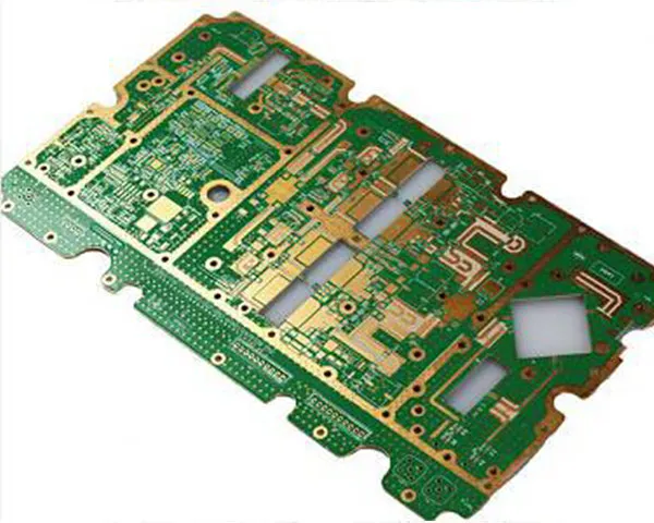
Above roughly 1 GHz a laminate stops behaving as a passive carrier. Dielectric loss arrives as attenuation, the dielectric constant sets the velocity of the signal and the length a stub may run, and moisture taken up from the air shifts both. A high-frequency board answers that with a material chosen for its electrical behaviour rather than its mechanical properties, and with a stack-up modelled before any copper is etched.
What changes above 1 GHz
- Loss — attenuation grows with frequency and with the dissipation factor of the laminate, so the material matters as much as the trace geometry.
- Dielectric constant — the trace width that gives a 50 Ω line depends on the dielectric constant and its tolerance, which is why the stack-up is fixed before routing.
- Moisture — absorbed water raises the effective dielectric constant and the loss, which is why the low-absorption laminates are used for equipment that works outdoors.
- Copper surface — at high frequency the current crowds into the surface of the conductor, so surface treatment and copper roughness are chosen with the finish, not after it.
- Mechanics — PTFE-based material is softer than FR-4, so drilling, hole treatment and panel support are adjusted for it rather than run on the standard recipe.
Materials and stock
Rogers, Arlon, Taconic and Nelco high-frequency laminates are held in stock, so a prototype does not wait on a material order; high-Tg FR-4 and halogen-free laminate cover the cases where the frequency is moderate and the budget is tighter. Boards are built from 1 to 38 layers up to 580 × 1900 mm, with 0.06 mm line and space on the fine-feature layers and 0.5–20 oz copper where a power section shares the stack-up.
Stack-up, impedance and assembly
Impedance is held to ±10 %: dielectric thickness, dielectric constant, copper weight and trace width are modelled together and then verified on the finished board. ENIG, immersion silver, immersion tin, flash gold, golden finger, HASL, lead-free HASL and OSP are all available, and mixed constructions are used where a digital section and an RF section share one board. Assembly runs in the same plant with four SMT lines at six million chips per day and X-ray inspection, so a populated RF module ships as one part.
Choosing the stack-up inside the RF range
A high-frequency request does not mean the whole board has to be built on the expensive laminate. The low-loss material has to sit where the attenuation, the dielectric constant or the absorbed moisture are actually in the signal path, and marking those layers is the first job in a stack-up review.
Two constructions cover most of the work. An all-high-frequency stack runs the same laminate through every layer, which keeps one press window and one expansion behaviour across the panel. A hybrid stack keeps the RF layers on the low-loss core and carries the digital and power layers on standard epoxy laminate, which buys the electrical performance where it is needed and leaves the rest on material that is easier to laminate and easier to buy. What the hybrid costs is a second material set and a second expansion behaviour, so the press cycle and the registration budget have to absorb both.
Inside the RF layers the trace width is not a free choice. The width that gives the target impedance follows from the dielectric constant and the dielectric thickness, so a thinner core pushes the lines narrower and a thicker core pushes them wider; the same width on a different laminate is a different impedance. Copper foil belongs to the same decision: rolled foil carries a smoother surface than electrodeposited foil, and at high frequency that roughness is part of the loss.
Four questions move the stack-up before anyone quotes it:
- The frequency together with the run length — a short run over a well-referenced layer can stay on standard laminate while a long run at the same frequency cannot, so the two are judged together and not by frequency alone.
- A continuous reference under the RF layer — the ground plane has to run unbroken beneath the trace, so a split that is harmless on a digital layer is a defect on an RF layer, and when the split cannot be removed either the routing or the layer count changes.
- Whether the board also has to fold or slide — a rigid-flex build carries the RF section across the hinge, and stacking more layers onto a rigid board does not.
- How many press cycles the stack needs — a hybrid or buried-layer stack is pressed more than once, and where that count comes from is set out on the multilayer PCB page.
None of this changes on its own. The stack-up fixes the drill program, the panelization, the coupon layout and the first-article checks, so it is settled in the engineering review before two quotations are put side by side.
Where high-frequency boards are used
Wireless and cellular infrastructure, satellite and radio equipment, radar and antenna modules, power amplifiers and low-noise amplifiers, and passive networks such as splitters, couplers, duplexers and filters. Automotive radar and telecommunications hardware are the volumes; where the temperature rather than the frequency is the hard requirement, a ceramic substrate takes over.
A 2026 case study shows how a 10-layer FR4 and Rogers RO3003 hybrid radar board was built for an automotive customer, with the lamination and impedance controls that made it possible.
What drives the price of a high-frequency build
Two quotations for one RF drawing can differ widely with neither supplier wrong, because the price follows how much of the low-loss laminate the design really needs, how many times the stack is pressed, and how the impedance coupons fall against the quantity — not the finished board area.
- The laminate is bought by sheet, not by board. A low-loss core carries a minimum order area and its own lead time, so a hybrid stack runs two material schedules at once and a small order is priced on the sheet it consumes rather than on the boards that come out of it.
- Offcuts stay with the order. High-frequency cores are panelized to the copper pattern of this job, and what is left over cannot be carried into another order as standard material, so utilisation is set by the panelization rather than by the board outline.
- The process window is narrower. A soft PTFE-based core needs its own drill parameters, its own hole treatment — plasma or sodium-naphthalene activation — and a different press profile, so the batch is set up for the material instead of running the standard recipe.
- Coupons and first articles ship with the batch. Dielectric thickness and dielectric constant are confirmed on a coupon that is cut and measured, so the verification is a fixed cost per batch and it lands on fewer boards as the quantity falls.
- A hybrid stack pays again at the press. Two materials expand by different amounts, so registration and yield move together, and the axis is settled by the stacked layers rather than by the vendor.
Comparability comes down to the same list in reverse: same laminate family, same stack-up, same foil type, same surface finish, same impedance target, same panelization and same quantity. The limits behind each of those axes are on the PCB manufacturing capabilities page.
Getting a quotation
Send the Gerber set with the laminate, the stack-up, the target impedance and tolerance, the frequency range and quantity. Prototypes come back in 1–3 days and medium volume in 4–10 days; process limits are on the capability page and the issued certificates on the certifications page.
High-frequency boards that move into assembly are covered on the China PCB assembly page, including sourcing and box build.