
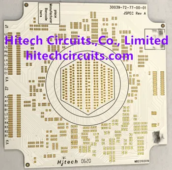
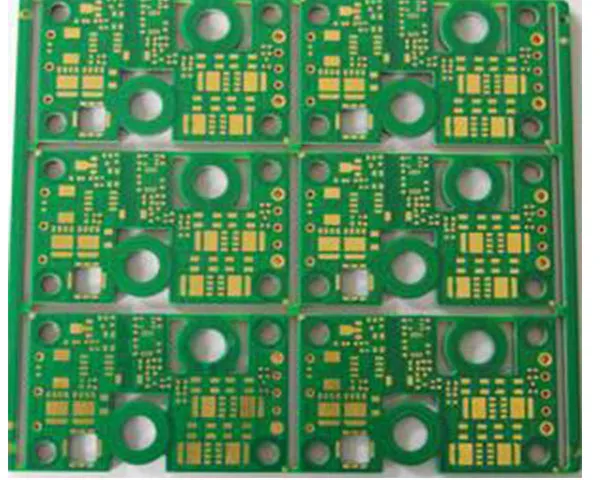
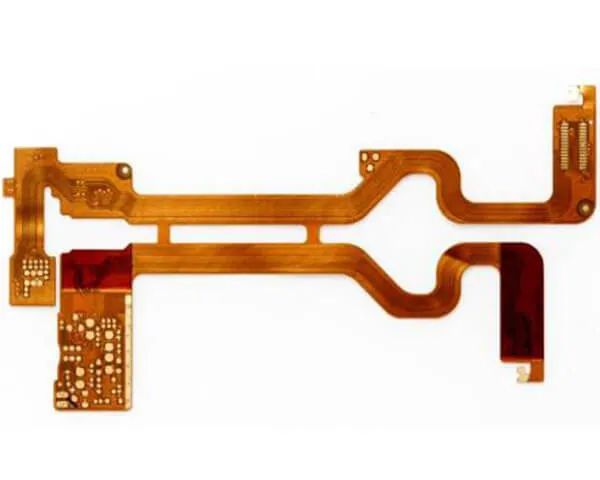
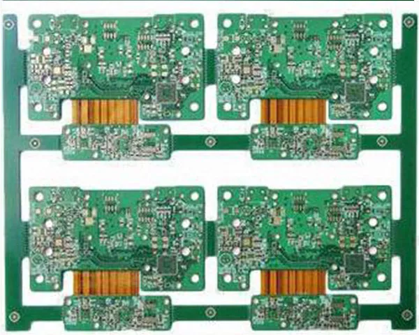
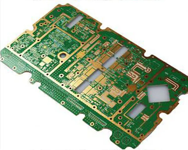

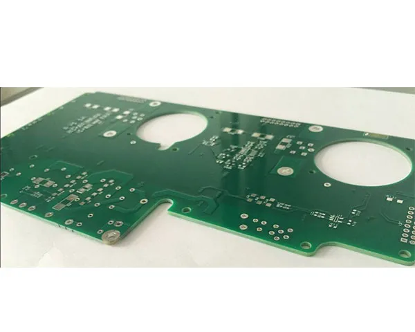
Printed circuit board manufacturing is the core of Hitech Circuits. Ten board families are produced in Shenzhen, and the limits behind them are published as numbers rather than adjectives: 1–38 rigid layers, 0.06 mm line and space, 0.1 mm laser-drilled vias, a 15:1 aspect ratio, outer-layer copper to 20 oz and panels up to 580 × 1900 mm.
What the plant fabricates
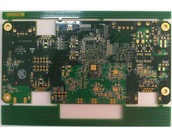
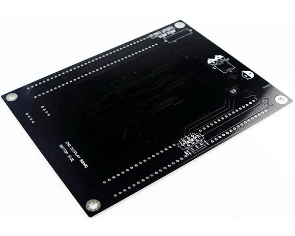
- Rigid and multilayer boards — 1–38 layers on FR-4, high-Tg FR-4, halogen-free laminate, CEM1 and FR-1, from a small prototype panel to 580 × 1900 mm production tooling.
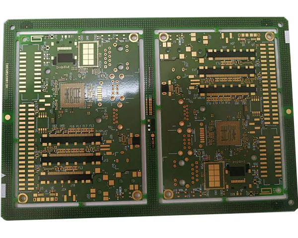
- HDI boards — 1+N+1, 2+N+2, 1+1+N+1+1 and 3+N+3 stack-ups with laser microvias and ELIC technology.
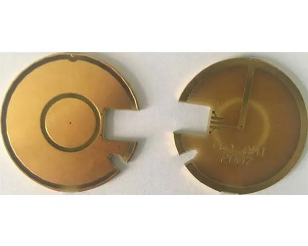
- Flexible and rigid-flex circuits — 1–12 layers on Kapton, PI and PET, bonded to FR-4 rigid sections, with 0.05 mm line and space and PI, PET, FR-4 or stainless-steel stiffeners.
- Metal-core boards — aluminium, copper and COB MCPCB constructions from 5 × 5 mm to 1900 × 480 mm, carrying 18–240 µm copper for LED, power and thermal designs.
- Ceramic substrates — 96 % and 98 % alumina, aluminium nitride and beryllium oxide in thin-film, thick-film and direct copper bonded processes, for designs from −55 °C to 850 °C.
- Heavy-copper, high-frequency and quick-turn builds — up to 20 oz outer copper, Rogers, Arlon, Taconic and Nelco laminates with impedance held to ±10 %, and prototypes inside 1–3 days.
The details that decide a quotation
Four points settle most of the risk in a design: layer count and minimum line width, copper weight, impedance tolerance, and the documentation a customer's own approvals need. All of them are reviewed in DFM, DFA and DFT before quoting, so stack-up, panelisation or clearance problems surface while they are still cheap to fix.
Surface finish is fixed together with the stack-up — HASL, lead-free HASL, ENIG, ENEPIG, immersion silver, immersion tin, flash gold, golden finger, OSP, carbon ink and peelable mask are handled in-house — and the full process limits sit on the PCB manufacturing capabilities page.
When the boards continue into assembly and box build, the China PCB assembly page covers how fabrication, component sourcing and assembly are quoted as one order.
When every limit passes and the combination does not
A capability table is read one row at a time, and a design can sit inside every row while the combination is still outside the process window. What a line opens and closes is a pair of features, and these are the pairs that come back from review most often.
- Fine lines on heavy copper. Etching takes copper off the top of a trace and off its side at the same time, so the thicker the layer the further the finished width drifts from the artwork. A line width that is routine on thin foil is a special job on a heavy layer, and asking for both at their extremes moves the board out of the standard window rather than to its edge.
- The smallest hole in the thickest board. Aspect ratio is a division, not a dimension: halving the finished hole doubles the ratio at the same thickness, and past a certain point the plating solution stops exchanging inside the barrel and the wall plates unevenly. A smallest-hole request and a thick-panel request are one decision, not two.
- A large outline on a thin board. Thin panels bow during etching, plating and pressing, and the larger the outline the further the flatness figures move, so a big thin board is judged on flatness before it is judged on features.
- Laser-drilled vias under heavy surface copper. A laser stops on the inner-layer pad it is aimed at, so the thicker or the more heavily plated that copper, the less forgiving the landing is and the more the HDI drill recipe has to be adjusted to it.
- Impedance targets after every press cycle. Each lamination closes the dielectric thickness to a tolerance and a coupon can only be measured afterwards, so a stack-up with more press cycles carries more chances for the target to drift — which is why controlled-impedance builds are settled at stack-up stage instead of corrected on the finished panel.
- Several finishes on one panel. A gold-finger edge, a solderable land and a carbon contact pad are three processes on one outline; each adds masking, a bath or a cure, so the board is priced as the sum of the routes it needs rather than as one route with extra steps.
A quotation is therefore written against the tightest pair in the enquiry, not against the most generous single figure. Naming which dimensions are fixed and which can move is worth more than reporting the extreme of every row, because relaxing one member of a pair is usually cheaper than asking the process to hold both. The capability page publishes the rows one at a time; the review is what puts them back together.
Bare board and assembly in one plant
Fabrication is only half the work. Four SMT lines place six million chips per day at 01005 and 0201 package sizes down to a 4 mil (0.1 mm) pitch, three DIP lines handle 1.6 million through-hole pieces per day, and BGA rework, re-balling and X-ray inspection cover the joints that cannot be seen. Cable and harness assembly and box build follow in the same building, so a product can ship as a built unit rather than as boards plus loose parts.
One quality system for every board type
ISO 9001:2015 is the base, with IATF 16949:2016 and ISO 13485:2016 layered on for automotive and medical work and ISO 14001 and ISO 45001 alongside them. Boards are fabricated to IPC-6012B and IPC-A-600H, UL recognised under file E354070 and RoHS compliant; the issued certificate scans are published on the certifications page.
Choosing between the eleven board families
A board is defined by what the design has to survive, and the family follows from that — these pages are not a catalogue to be read in order.
- A board that has to bend or fold belongs to flex and rigid-flex, where the bend radius and the stiffener layout shape the stack-up instead of the layer count.
- Density rather than area pushes a design into HDI once the escape routing under a fine-pitch package no longer fits the layers a standard panel can carry.
- Heat that has to leave through the board goes to metal-core or ceramic work; current that has to travel through the copper goes to heavy copper. Both follow from a thermal or a current figure, not from a preference for a laminate.
- Frequency and ambient temperature narrow the laminate list before any mechanical question is asked, which is why high-frequency and ceramic enquiries are reviewed against the stack-up first.
- A design that outgrows two layers moves to multilayer for interconnect density, not for the sake of a higher layer count.
Not every one of the eleven pages is a material family: the double-sided page describes the plainest two-layer interconnect, and the heavy-copper design guide is a method document rather than a product. All families run on the same lines, so a design that moves from one to another keeps its supplier — but it changes its stack-up, its tooling and its price.
What separates a prototype run from a production run
The same Gerber set is quoted on two different cost lines depending on quantity, and the differences that matter are structural rather than technical.
- Panelisation is paid once or on every board. A prototype goes onto a standard panel size; a production order is panelled to the customer's outline, and the area lost outside that outline is paid on every panel of the run.
- The stack-up comes from a standard library or gets built. Standard FR-4 builds go straight onto the line; a custom build is pressed and cross-sectioned first, and that trial belongs to the order that triggered it.
- A specialist laminate is bought by the pack. A high-frequency or ceramic order carries the maker's full pack whether or not the panel uses all of it, so a small quantity pays for material it does not consume.
- Quality documents are batch costs. First-article reports, microsections and impedance coupons are produced per batch, which makes them a large share of a small order and a small share of a large one.
A quotation therefore prices a batch rather than a board, and the per-board figure moves with the quantity even where nothing in the design has changed.
What happens between a Gerber set and a production program
An order does not travel straight from a customer's files to a drill bit. A front-end step turns artwork into tooling first, and most of what a fabrication quotation asks about belongs to that step rather than to the design.
- The artwork carries no nets. A Gerber set describes copper shapes; it does not say which shapes form one circuit. Electrical test is programmed from a netlist, so a job built from artwork alone is proven for continuity between what the drawing shows, not for the connectivity the designer intended. Sending the netlist with the files is what makes the test coverage mean something.
- The panel is what is processed. Tooling strips, location holes, fiducials and the route path live on the panel rather than on the board, and the way the outlines are packed decides how many cuts a board needs and which handling the batch gets.
- The artwork is compensated before it is imaged. Etch compensation widens or narrows drawn features so the finished dimension lands where the drawing says, mask openings are grown to keep the web between pads, and legend is checked against what the printer can hold. The film on the line is not the file that arrived.
- The stack-up is solved backwards from the target. Controlled impedance is a result, not an input: the line width and dielectric thickness that produce the target are calculated from the laminate's properties, and the answer can differ from the stack-up the drawing shows. That is why impedance questions arrive before the quotation instead of after the first article.
- Questions come back on purpose. The front end returns a list rather than a price when an annular ring, a hole-to-copper distance, a mask web or a test point cannot be built as drawn — and each of those is cheap while the order is still a file.
None of it changes the layout intent; it decides what the layout becomes on the floor. A file set that arrives with its netlist, its stack-up intention and its quantities leaves the front end with little to ask, and an unanswered question is paid for per panel rather than per reply.
How to start
Send the Gerber set or the BOM — or both — with the stack-up, quantity and target date. Prototypes come back in 1–3 days and medium-volume boards in 4–10 days, with stencils cut and delivered within four hours; mass production is scheduled once the BOM is released. The same board types are rebuilt for different markets, and the industries pages show what changes in each vertical.