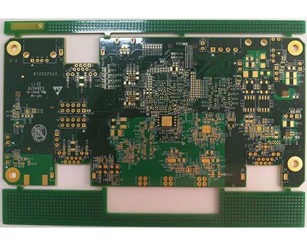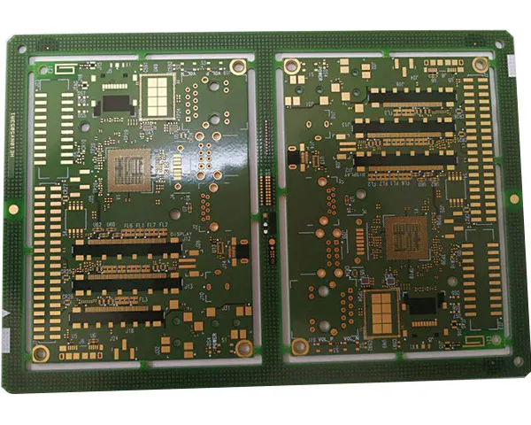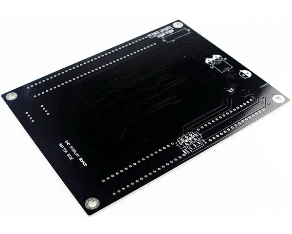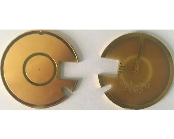
A double-sided board carries copper on both faces and joins the two layers with plated through-holes. It is still the workhorse of the assembly industry: the layer count keeps the price down, the second copper layer frees the routing, and the design rules are the same ones a 38-layer board is held to, because both come off the same line.
What the second layer buys
- Routing room — a two-layer board can cross conductors instead of routing around them, so a dense control section fits without adding layers.
- Ground and power planes — the second face carries a solid plane, which shortens the return path and removes the loop area that a single-sided layout leaves open.
- Component density — parts can be placed on both sides, which halves the outline where the enclosure is the constraint.
- Cost — two layers avoid the lamination cycles of a multilayer build while keeping impedance controlled to ±10 % where the stack-up needs it.
Materials and panel sizes
FR-4 is the standard core, with high-Tg FR-4 for higher soldering temperatures, CEM1 and FR-1 for cost-driven consumer work and halogen-free laminate where the customer's own approvals ask for it. Panels run up to 580 × 1900 mm and 0.1–6.0 mm thick, with copper from 0.5 oz to 20 oz on the outer layers — a 20 oz two-layer board is a common way to carry a heavy current without going to a heavy-copper stack-up.
Process and inspection
Boards are drilled mechanically from 0.15 mm or by laser to 0.1 mm, plated, imaged at 0.06 mm line and space, then finished in HASL, lead-free HASL, ENIG, immersion silver or tin, flash gold, golden finger, OSP or carbon ink. Outline is held to ±0.10 mm and bow and twist to 0.7 %; every panel is electrically tested before shipment, and boards are fabricated to IPC-6012B and IPC-A-600H with UL recognition under file E354070.
Where two-layer boards are used
Industrial control and relay logic, power supplies, LED lighting and drivers, consumer electronics, instrumentation and telecommunications equipment. Double-sided reflow allows both faces to be populated, which keeps the outline small in wearable and handheld products; where the design needs microvias rather than through-holes, the same panel can be built as an HDI board.
When two layers are the wrong answer
A two-layer board stops being the cheap answer as soon as the design asks for something the two copper faces cannot deliver. The signals show up on the drawing rather than in the quotation, and each one changes the board type instead of the board price.
- The reference plane can no longer stay continuous — the second face has to carry routing and plane at the same time, so every trace that crosses cuts the return path underneath it. Once a controlled-impedance line, a differential pair or a fast bus has to hold its impedance from driver to receiver, an uninterrupted plane is worth more than the lamination it costs; how the layers are then assigned is covered under Multilayer PCBs.
- Heavy current and fine pitch pull in opposite directions — etching a thick foil undercuts the trace from the side, so the heaviest copper and the finest line and space cannot be produced on one panel at the same time. Splitting the board into a power zone and a logic zone keeps both, but where the current itself is the requirement the answer is a Heavy Copper PCBs with a different etch budget.
- The escape runs out before the routing starts — a fine-pitch BGA or a high pin-count connector can exhaust the room between its pads before the first signal is drawn, and no amount of cross-layer routing recovers it. That is a via question rather than a layer question, so the same panel is rebuilt with microvias instead of through-holes.
- The assembly has to fold — a board that hinges, slides or wraps around a housing was never a two-layer problem; Rigid-Flex PCBs covers the construction that replaces the connector and the cable the assembly would otherwise need.
- The second layer ends up as a plane only — if the routing fits on one face and the second face is spent entirely on ground, the design is paying for a layer it does not use.
Changing the board type is not adding a layer: the outline, the panelisation, the stencil apertures, the programmes and the first article all follow the new stack-up. The decision belongs in the DFM review, while the drawing is still open, and not in the comparison between two quotations.
What actually sets the price of a two-layer board
Two boards with the same outline and the same layer count can quote far apart without either supplier being wrong. On a two-layer panel the price is set by the work the features demand, and the layer count is only the entry ticket.
- Hole count and aspect ratio — every through-hole is drilled, plated, inspected and electrically tested, so the number of holes carries the drilling and plating time of the panel. Depth against diameter decides how hard the drill has to work, and a broken drill in a deep small hole costs the panel rather than the hole.
- Copper weight against line width — the same undercut that limits fine line on a heavy foil also limits how much copper can be added to a fine-line layout; a panel is either split into zones or quoted against the heavier of the two requirements.
- Panel utilisation and process edge — the price follows the panel area and the number of up-sites, not the finished outline. The spacing between boards and the process edge are consumed by the tooling, and squeezing the geometry does not recover them.
- Laminate, Tg and stock — the difference between a standard laminate and a high-Tg or halogen-free core is a press window and a stock position rather than a weight of material, and a laminate that has to be ordered in changes the lead time before it changes the price.
- Surface finish and contact requirements — HASL, lead-free HASL, immersion finishes, ENIG and hard gold on a chamfered edge are different processes on the same copper, and the choice is set by how the pad is soldered, contacted and stored, not by habit.
- Profile and tooling — a routed outline follows the drawing, a V-cut works only in a straight line, and a punched profile needs a die that a short run cannot absorb.
Two quotations are comparable only when the laminate, the copper weight, the surface finish, the panelisation, the quantity and the electrical test coverage are the same; where one of them differs, the cheaper board is a different product rather than a better price.
Getting a quotation
Send the Gerber set with the layer count, copper weight, surface finish, panel size and quantity. Prototypes come back in 1–3 days and medium volume in 4–10 days, with stencils cut within four hours; the capability page holds the process limits used for the quotation and the certifications page the issued certificates.
When the double-sided boards move into assembly, the China PCB assembly page covers SMT, through-hole, component sourcing and box build from one plant.