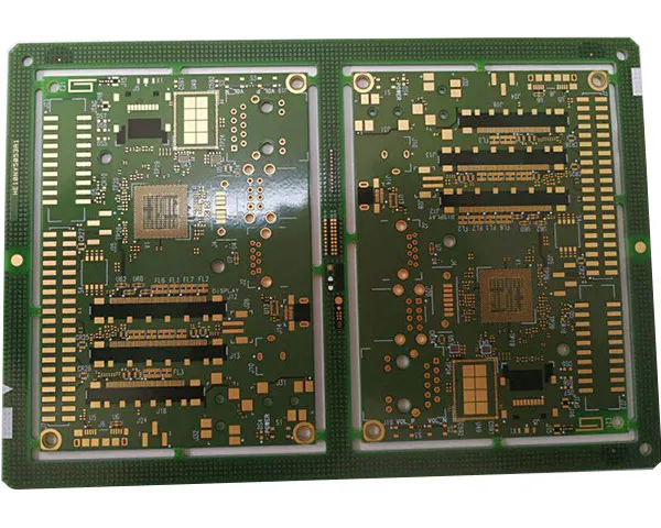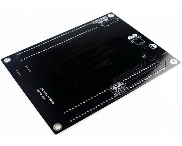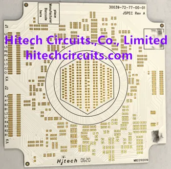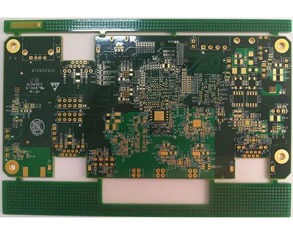
A multilayer PCB presses two or more inner conductor layers between insulating plies, then connects them to the outer layers with plated holes. The result is more routing in the same footprint, a solid reference plane under high-speed signals, and a shorter path between power and ground — which is why almost every product with a processor, a radio or a dense connector moves past two layers quickly.
Single-sided, double-sided and multilayer
- Single-sided — one copper layer, holes for through-hole parts only. Suitable for the simplest circuits and the lowest cost.
- Double-sided — copper on both faces, connected through plated holes, which carries the majority of small products.
- Multilayer — three or more conductor layers, inner layers processed before lamination and the outer layers afterwards. Hitech Circuits builds these from 4 to 38 layers, with 0.06 mm line and space and outer copper from 0.5 oz to 20 oz.
How the board is built
Inner layers are imaged, etched and inspected, then laminated under heat and pressure with the prepreg that sets the dielectric thickness between them. Drilling follows the stack-up: 0.15 mm mechanical holes and 0.1 mm laser holes with a 15:1 aspect ratio, copper plated to the inner layers, outer layers imaged and etched, then solder mask, surface finish and profile routing. Board thickness is held to ±8 % at 0.8 mm and above and ±10 % below that, with outline tolerance of ±0.10 mm and bow and twist inside 0.7 %.
Stack-up, impedance and materials
FR-4 covers most builds, with high-Tg FR-4 for boards that see repeated thermal cycling, halogen-free laminate where the customer's own approvals require it, and Rogers, Arlon, Taconic or Nelco where the signal has to survive at high frequency. Impedance is calculated from the stack-up and controlled to ±10 % — the same review fixes panelisation and copper balance so the finished panel does not bow. Where density rather than layer count is the constraint, microvia stack-ups from HDI boards are built on the same floor.
Typical multilayer builds
Four, six and eight layers carry most of the work, and the stack-up follows the job: the layer count is set by routing density, the number of planes and the current that has to be carried, not the other way round.
- 4-layer control boards — signals on both outer layers with a ground plane and a power plane inside; the lowest-cost way to put a solid reference plane under a microcontroller or a fieldbus transceiver.
- 6- and 8-layer power boards — a power section that shares the stack-up with its own control logic, using 0.5–20 oz copper on the outer layers and 0.5–10 oz inside, so a heavy-current path and a 0.06 mm logic layer are etched on the same panel.
- High-speed networking and measurement boards — where loss rather than copper weight sets the limit, the build moves onto high-frequency laminate (Rogers, Arlon, Taconic, Nelco) and the stack-up is fixed before routing; the high-frequency PCB page covers the material side of that choice.
- Mixed digital and power — impedance held to ±10 % on the controlled layers while the heavier layers carry current, both reviewed in DFM so panelisation and copper balance stay inside 0.7 % bow and twist.
All four run on the same line as single-sided and double-sided boards, so a prototype and the production panel are held to the same 0.06 mm line and space and the same ±10 % impedance tolerance.
Choosing the layer count inside the multilayer range
A multilayer request rarely arrives as a number of layers. It arrives as constraints — how much has to be routed, how thick the finished board may be, and whether a hole has to stop at an inner layer — and the layer count is what those constraints add up to. Two versions of the same product can be built on noticeably different stacks and both work; what separates them is where the reference planes sit, not the number written in the title block.
The rule that fixes most builds is one plane for every signal layer. A four-layer board is two signal layers with a power plane and a ground plane inside, a six-layer board is four signal layers between the same pair of planes, and an eight-layer board is six signal layers with the pair at the middle. Above that the pattern repeats, and the useful questions move elsewhere: whether the return current can stay under the trace it belongs to, and whether the planes can be shared.
Sharing a plane is cheaper than adding one. One ground plane can serve a digital section and an analogue section, and one power plane can feed several rails, as long as the return current never has to cross a slot and the decoupling loop stays short. While both hold, the split is a layout decision; when either fails, the answer is another plane, and only then another layer.
Thickness is where most layer-count plans meet the laminating window. Finished thickness divided by the layer count is the dielectric left for each layer, and thin cores and thin prepreg stop being pressable before they stop being affordable. A high layer count inside a slim profile asks for a stack the press cannot hold, so either the finished board grows or the count comes down — arithmetic that belongs to the stack-up review, not to the quotation.
Four questions move the count in practice:
- Impedance that has to hold across the board, under a bus or a differential pair — a continuous reference has to sit under the trace, which is what turns two layers into four or six, whatever routing is left over.
- Two supplies plus ground plus dense routing on one board — six or eight layers, where the extra pair buys separated planes rather than more area.
- Holes that stop at an inner layer — blind and buried vias need more than one press cycle, so the comparison is thinner dielectric on through-holes first, extra layers second.
- A board that also has to fold or slide — a rigid-flex build carries the stack across the hinge instead of adding layers to a rigid board.
None of these changes on its own. The stack-up fixes the finished thickness, the panelization, the drill program and the first-article checks, so it is settled in the DFM review before two quotations are put side by side.
Where multilayer boards are used
Communications equipment, industrial control, GPS and satellite units, aerospace, computing, medical devices, military hardware — and the telecom and network hardware described on the telecommunications page. Boards for vehicles follow IATF 16949:2016 and medical boards follow ISO 13485:2016, both on top of the base ISO 9001:2015 system; fabrication runs to IPC-6012B and IPC-A-600H with UL recognition under file E354070.
A 2026 case study shows a 10-layer board that hybrid-laminates FR4 Tg180 with Rogers RO3003 for a 77 GHz automotive radar.
What drives the price of a multilayer build
Two quotations for one multilayer drawing can differ widely with neither supplier being wrong, because the price follows how many times a panel is pressed and how many usable boards come out of one inner-layer sheet, not the finished area alone.
- Every press cycle costs its own material set, its own press program, its own registration check and its own thickness measurement. A build that needs more than one pass is a different process, and it is priced as one.
- Scrap multiplies down the sequence. A fault found after the first press takes the inner layers with it, so the loss is the artwork, the copper and the work already inside the panel rather than a single sheet; a high layer count forgives fewer mistakes, and the price carries the average.
- Inner sheets are panelized to the copper pattern and to copper balance, not to the finished outline, so price follows how many boards leave one sheet rather than the board size in the drawing.
- An asymmetric stack is brought back into balance with dummy layers or a different build, and uneven copper gets thieving; both are layout decisions taken before material is ordered, and both change what the panel costs.
- Pairing a high-frequency core with a standard outer laminate means two material sets, two press windows and two expansion behaviours, which moves lead time and yield together.
Comparability comes down to the same list in reverse: same stack-up, same number of press cycles, same laminate set, same surface finish, same panelization and same quantity. The limits behind each of those axes — layer count, panel size, press cycles — are on the PCB manufacturing capabilities page.
Getting a quotation
Send the Gerber set, the stack-up or layer count, copper weight, impedance requirements and quantity. Prototypes come back in 1–3 days and medium volume in 4–10 days; the capability page lists the limits behind the quotation and the certifications page holds the issued certificates.
Multilayer boards that continue into assembly are quoted with component sourcing and box build on the China PCB assembly page.