Why a board gets reverse engineered
Three cases account for most reverse engineering work: the drawings no longer exist, the original manufacturer has stopped supporting the product, or a board from your own fleet has to be understood before it can be repaired or requalified. In all three the target is the same — a documentation set you can build from, not a copy of somebody else's design.
What can be recovered, and what cannot
Recovered with confidence: layer count and stack-up order, copper geometry per layer, the drill table, mask and legend openings, the netlist, and the position and orientation of every package.
Inferred, then verified: component values where the markings survive, and the function of each block once the netlist is readable.
Not recoverable from the board alone: firmware, the exact part number behind a potted or laser-etched device, and any parameter that only ever existed in the original vendor's BOM. A supplier who promises a complete recovery is describing a copy, not an analysis.
The working sequence
- Log the board — photographs of both sides with a scale, and a written record of every marking before anything is removed.
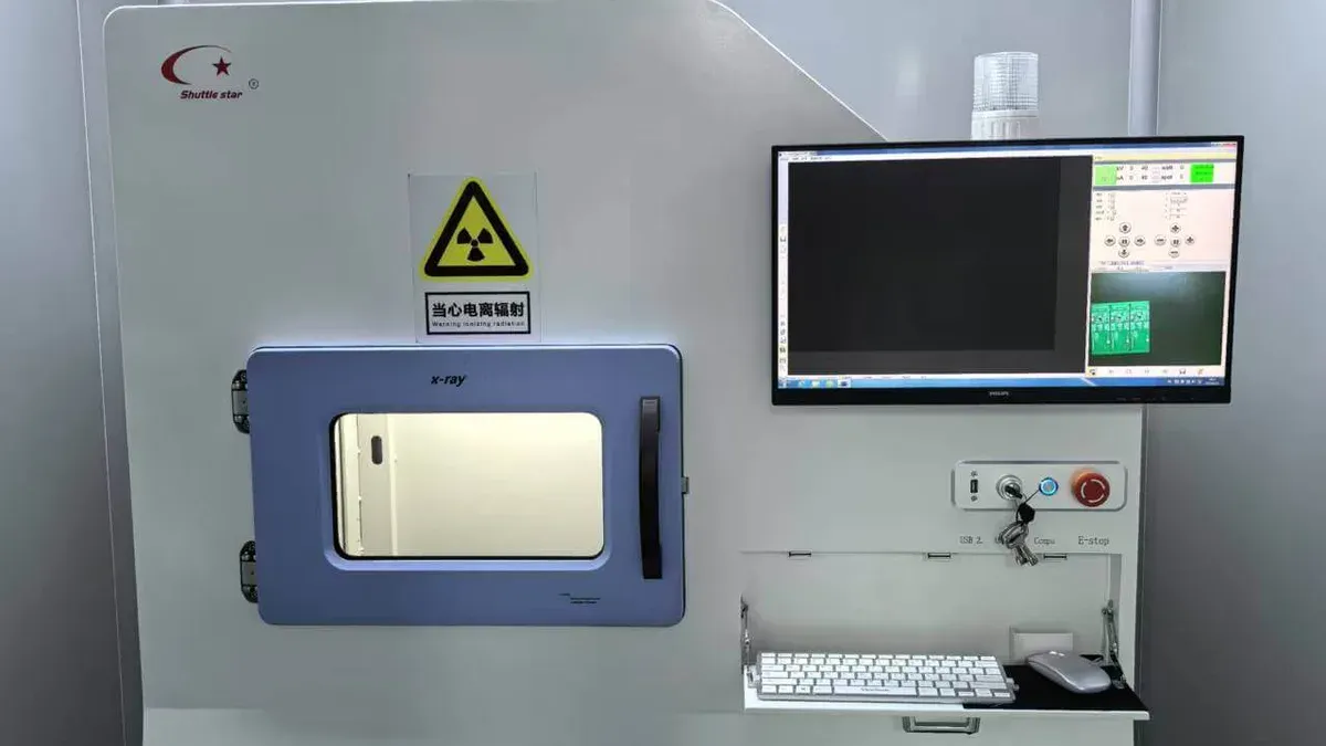
- X-ray the board — layer count, plane layers, via types and internal registration. This step decides the cost of everything after it; the X-ray is the same tool described in Six Ways to Inspect a PCB Assembly, pointed here at the stack rather than at the joints.
- Strip what covers the copper — conformal coating, potting, and where necessary the components themselves.
- Delayer and scan — the board is milled back one layer at a time and every copper layer is scanned at high resolution.
- Rebuild the netlist — scanned layers are vectorised and cross-checked against each other. A net that appears on one layer but not in the rebuilt file is treated as a rebuild error and re-checked against the physical board before it is accepted.
- Rebuild the schematic by block — power, digital, analog, interface. Blocks are named by function, because the original names were never printed on the board.
- Verify against the physical board — probe the original where the netlist is ambiguous, then build a first article from the rebuilt data and test it.
Deliverables
A typical documentation set contains:
- Schematic, as PDF and as an editable source file
- Netlist and BOM, with alternates named where the original part is obsolete
- Gerber and drill file at 1:1, in a format a fabrication house can run without conversion — the same data set a PCB Manufacturing order is quoted from
- Stack-up drawing with copper weight and dielectric build for each layer
- Test list and test-point map for the rebuilt assembly
Where the limits come from
The first limit is optical: a fine-pitch BGA whose traces run under the package can only be read after the device is removed. The second is material: potting, heavy copper and thick laminates all cost scan time. The third is scale — a two-layer board can often be rebuilt from photographs, while a high-density board with laser vias cannot.
Where the rebuilt data goes back into production, it has to fit the fabricator's published window — here, 1–38 layers at 0.06 mm line and space — so that number is worth checking before the first scan rather than after it. Those limits are listed on the PCB Manufacturing Capabilities page.
Ownership, NDA and what a lab should refuse
Ownership comes before tooling. The board should either belong to the customer or be covered by written authorisation to reproduce it, and an NDA should be in place before the board changes hands. Work to clone a competitor's product for resale, to remove a competitor's label, or to copy a design whose ownership is unclear is not something a legitimate lab should quote for. If the board is still under warranty from another maker, raise it at quotation stage — it changes which route is sensible.
What drives the cost
Layer count and board area set the number of scans. The count of unique nets sets the schematic time. Desoldering and measuring parts adds a stage, and electrical verification on the rebuilt first article adds another. A quotation is itemised along those lines, which is why two boards of the same size can land on very different prices.
What a quotation request should contain
A quotation request needs photographs of both sides, the layer count if it is known, the target deliverable, and the end use of the product. If the board is still inside an assembly, say so — the housing, connectors and cable form often carry information the bare board does not. Where the rebuilt board then goes into production, the gates it will pass through are described in the quality control gates note.