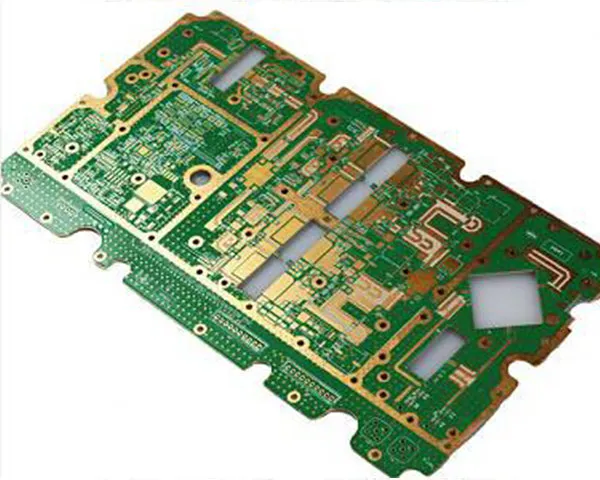
ALPHA is a German family-owned EMS company founded in 1985 and based near Darmstadt, working in medical electronics and the high-end niche markets around it. In 2025 it took on a new-generation remote medical sensing controller, and the board that carries the controller sets the bar for the whole programme: an 8-layer, 2+N+2 HDI design with BGA packages and an ENIG finish, specified for signal integrity and long-term reliability.
The programme
The board is hard on its own. A 2+N+2 stack-up at 0.06 mm line and space leaves a narrow process window at imaging and etching, and the BGA joints are hidden, so soldering has to be controlled by process rather than inspected by eye. A single error at any stage can become a batch rework. The validation window was also short — the controller had to reach working prototypes quickly so it could go into end-customer evaluations.
Why one supplier
ALPHA had been buying PCB fabrication, component sourcing, SMT, PCBA functional testing and the stages between them from separate suppliers. Every handover added communication and lost schedule, and responsibility changed hands at the points where defects are easiest to introduce. The brief was therefore not just a board but a single window: Gerber and BOM in, finished and tested boards out.
What engineering changed on the line
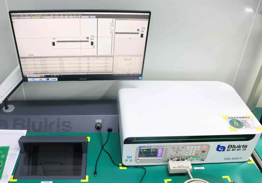
HITECH CIRCUITS ran a DFM review before production and returned the report within 24 hours, with optimisation suggestions that removed two potential soldering risks from the design. For the BGA joints the team set the stencil apertures and the reflow profile, then checked the result with X-ray sampling so each joint was inspected for insufficient solder and bridging; AOI and a functional test added the second layer of verification.
Long-lead BGA material was locked in as soon as the sample PCBA order arrived, so procurement did not sit behind the board. Fabrication and assembly then ran in sequence — material cut, lamination, PTH, solder mask, ENIG and electrical test, followed by component sourcing, SMT, SPI, AOI, X-ray and functional test — without a supplier handover in the middle.
Delivery
The delivery commitment was written into the cooperation agreement: samples in 10 days, batch completion in 3 weeks. The samples shipped on the agreed date.
Customer feedback
When the PCBA samples arrived, ALPHA reported that the control mainboard exceeded its expectations, that the BGA soldering was clean and that every functional test passed. It said the delivery date had been met to the letter — rare in its procurement experience — and confirmed that the batch order would stay with HITECH CIRCUITS, with more of its product lines expected to follow.
What it shows
The programme combined three things that are usually bought from different suppliers: one-stop PCBA (sourcing, fabrication, assembly and test under a single order), process capability on a 2+N+2 HDI board with BGA packages, and a delivery date that was agreed and kept. For a buyer comparing suppliers, the useful question is not the layer count alone but whether the same partner can carry the board from Gerber to tested unit without losing the schedule in between.
The process limits behind the build are on the capability page; the board family has its own page on HDI; the assembly scope is described under turnkey electronics assembly; and the industry context sits on the medical equipment page. To start a similar programme, send the Gerber set, BOM and target date on the contact page.